
Arun Pratap S. Rathod
Department of Electronics and Communication Engineering, Graphic Era Hill University, Dehradun, India
Pawan K. Mishra
Department of Computer Science & Engineering, Graphic Era Deemed to be University, Dehradun, Uttarakhand, India.
Keywords: Multiplexer OTFT Organic electronics Thin films CMOS OTFM
Abstract
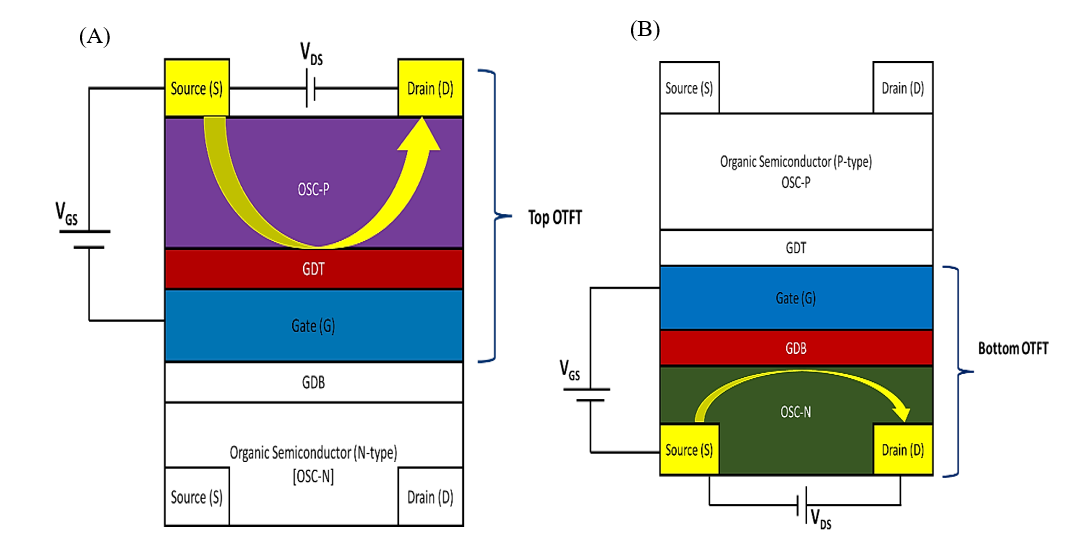
In recent years a transition from conventional electronic devices based on silicon to organic material based electronic devices has been observed. As the market for flexible and wearable devices has presented greater opportunities and sharp growth, the demand for organic thin film transistor (OTFT) based combinational circuits has increased exponentially. Traditionally such circuits were fabricated through complementary metal oxide semiconductor (CMOS) logic architecture, but due to large number of nodes OTFTs employed in circuit implementation, the overall power consumption, interconnect delay and the chip area of the circuit increases significantly. Organic thin film multiplexer (OTFM) is a novel attempt to redesign an existing multi-transistor combinational logic device like 2:1 Multiplexer in the form of a single multi-layered logical device, while maintaining the dimensions, material composition and fabrication method equivalent to single OTFT (bottom gate bottom contact OTFT). The design and development of the OTFM has been achieved through Silvaco a large ion collider experiment (ATLAS) technology computer-aided design (TCAD) tool while the examination of power and area consumption of the OTFM and equivalent CMOS circuit was accomplished through post layout (physical design) analysis using Cadence Virtuoso exploratory data analysis (EDA) tool. It has been found in this research that the power and chip area consumption of proposed OTFM is lower than that of CMOS logic based 2:1 Multiplexer by 90% and 95% (approx.) respectively, while operating under same voltage regime for implementing identical logical functions.
How to Cite
Rathod, A. P. S. ., & Mishra, P. K. . (2025). Design and analysis of novel organic thin film multiplexer . Asia-Pacific Journal of Science and Technology, 30(06), APST–30. https://doi.org/10.14456/apst.2025.88
References
Kumar B, Kaushik BK, Negi YS. Perspectives and challenges for organic thin film transistors: Materials, devices, processes and applications. J Mater Sci Mater Electron. 2014; 25(1):1-30.
Cantatore E, et al. A 13.56-MHz RFID system based on organic transponders. IEEE J Solid State Circuits. 2007; 42(1):84-92.
Yunusa Z, Hamidon MN, Kaiser A, Awang Z. Gas Sensors: A Review. Sens. Transducers. 2014; 168:61-75.
Ong BS, Wu Y, Liu P, Gardner S. High-Performance Semiconducting Polythiophenes for Organic Thin-Film Transistors. J Am Chem Soc. 2004; 126(11):3378-3379.
Horowitz G. Organic Field-Effect Transistors. Adv Mater. 1998; 10(5):365-377.
Lee JH, Lee MH, Park JH. Design and characterization of low-power organic thin-film transistor-based digital circuits. J Semicond. 2022; 43(4):042601.
Gelkop B, Aichnboim L, Malka D. RGB wavelength multiplexer based on polycarbonate multicore polymer optical fiber. Opt Fiber Technol. 2021; 61:102441.
Menahem J, Malka D. 1 × 4 wavelength demultiplexer c-band using cascaded multimode interference on SiN buried waveguide structure. Mater. 2022; 15(14):50-67.
Menahem J, Malka D. A two-channel silicon nitride multimode interference coupler with low back reflection. Appl Sci. 2022; 12(22):11812.
Gindi M, Melamed A, Malka D. A four green-light demultiplexer using a multi gallium nitride slot-waveguide structure. Photon Nanostruct Fund Appl. 2020; 42:100855.
Sitbon E, Ostrovsky R, Malka D. Optimizations of thermo-optic phase shifter heaters using doped silicon heaters in Rib waveguide structure. Photon Nanostruct Fund Appl. 2022; 51:101052.
Isakov O, Frishman A, Malka D. Data center four-channel Multimode. Integr Multiplexer Using SiN Technol. 2024; 14(6): 60486.
Krause EE, Malka D. Optimizations of double titanium nitride thermo-optic. phase-shifter heaters using SOI technology. Sensors. 2023; 23(20):8587.
Chandrakasan AP, Kang SM, Bowhill WJ. Minimizing power consumption in digital CMOS circuits. Proc IEEE. 1995; 83(4):498-523.
Kumar B, Kaushik BK, Negi YS. Organic thin film transistors: Structures, models, materials, fabrication, and applications: A review. Polym Rev. 2014; 54(1):33-111.
Klauk H. Organic thin-film transistors. Chem Soc Rev. 2010; 39(7):26-43.
Cui H, Huang Y, Feng H, Song Y, Zhou D, and Li C. Design and performance optimization of organic thin-film transistors-based multiplexer. IEEE Trans Nanotechnol. 2021; 20(6):815-819.
Wondmagegn W, Pieper R. Simulation of top-contact pentacene thin film transistor. J Comput Electron. 2009; 8(1):19-24.
Ishikawa Y, Wada Y, Toyabe T. Origin of characteristics differences between top and bottom contact organic thin film transistors. J Appl Phys. 2010; 107(5):053709.
Klauk H, Zschieschang U, Halik M. Low-voltage organic thin-film transistors with large trans conductance. J Appl Phys. 2007; 102(7):074514.
Kudo K, Sakanoue T, Ishikawa K, Nakayama Y, Sakurai T, Someya T. Simulation framework for organic transistor circuits. IEEE Trans Electron Devices. 2018; 65(1):274-280.
Maiti TK, Chen L, Zenitani H, Miyamoto H, Miura-Mattausch M, Mattausch HJ. Physically based compact mobility model for organic thin-film transistor. IEEE Trans Electron Devices. 2016; 63(5):2057-2065.
Chen CH, et al. The interplay of thermal, time and Poole-Frenkel emission on the trap-based physical modeling of GaN HEMT drain characteristics. IEEE Compd Semicond Integr Circuits Symp. 2017; 95(11): 1-4.
Wu WJ, Yao RH, Li SH, Hu YF, Deng WL, Zheng XR. A compact model for polysilicon TFTs leakage current including the poole-frenkel effect. IEEE Trans Electron Devices. 2007; 54(11):2975-2983.
Fugazza D, Ielmini D, Lavizzari S, Lacaita AL. Distributed-Poole-Frenkel modeling of anomalous resistance scaling and fluctuations in phase-change memory (PCM) devices. IEEE Int Electron Devices Meet. 2009; 90:1-4.
Deen MJ, Marinov O, Zschieschang U, Klauk H. Organic thin-film transistors: Part II—parameter extraction. IEEE Trans Electron Devices. 2009; 56(12):2962-2968.
Mittal M, Rathod APS. Digital circuit optimization using pass transistor logic architectures. Int Conf Emerg Trends Commun Technol. 2016;5: 1–5.
Rathod AP, et al. Design and analysis of central gate organic thin film transistor. Eng Res Express. 2024; 6:045317.
Ling MM, Bao Z. Thin film deposition, patterning, and printing in organic thin film transistors. Chem Mater. 2004; 16(23):4824–4840.
Klauk H, Zschieschang U, Halik M. Low-voltage organic thin-film transistors with large transconductance. J Appl Phys. 2007; 102(7):074514.
Zhang XH, Domercq B, Wang X, Yoo S, Kondo T, Wang ZL, Kippelen B. High-performance pentacene field-effect transistors using Al₂O₃ gate dielectrics prepared by atomic layer deposition (ALD). Org Electron. 2007; 8(6):718–726.
Published: Nov 3, 2025
License
This work is licensed under a Creative Commons Attribution-NonCommercial-NoDerivatives 4.0 International License.